Sold out. We can let you know when it is available.
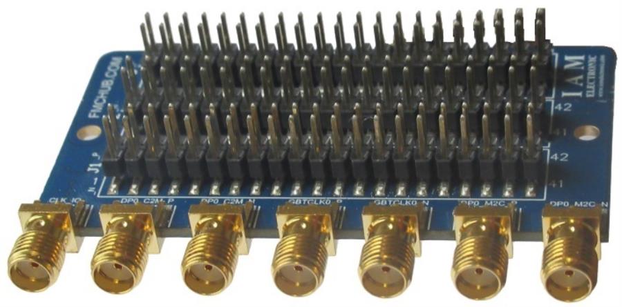
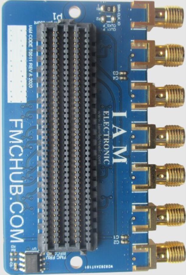
The FMC pin header board was developed to make the high density FMC connector of many FPGA boards easily accessible.
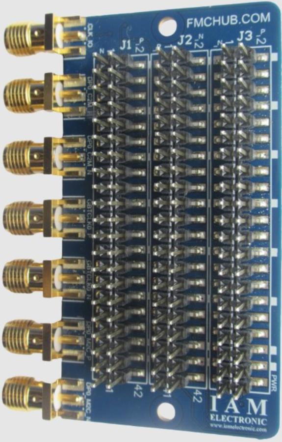
In many applications easily pluggable connections are required to process and check the digital signals. The use of 2.54 mm pin headers is very common.
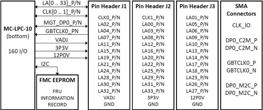
Thus, the FMC pin header board enables a variety of applications for digital signal processing and testing. The total number of 68 user signals (LAxx_P/N), 4 user clocks (CLKx_M2C_P/N) and 3 voltage rails (VADJ, 3P3V and 12PV0) from the carrier card connector are routed to the 2.54 mm pin grid on top of the adapter board.
In addition, the high-speed data lanes (multi-gigabit transceivers) are easily accessible via SMA connectors on the edge of the PCB. Finally, the board allows complete interconnection of all signals from the FMC connector.