Sold out. We can let you know when it is available.
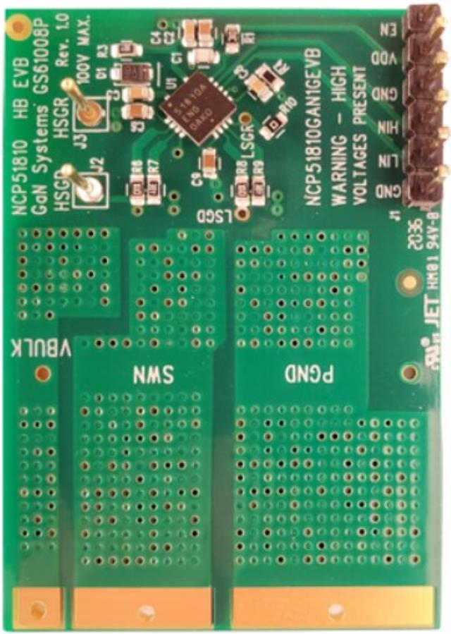
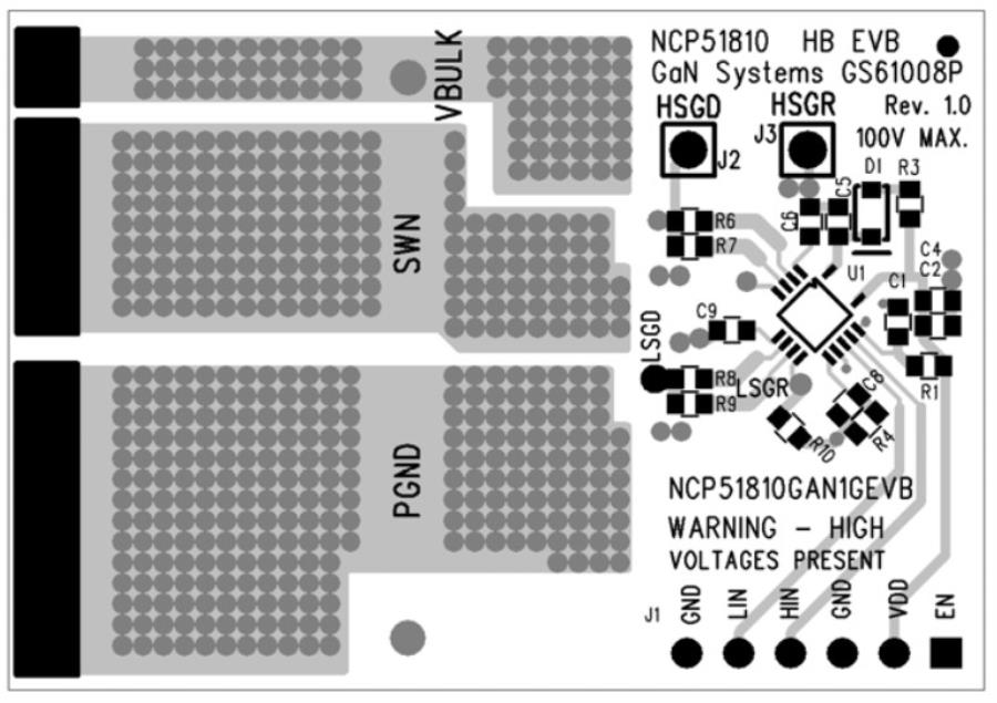
The NCP51810 HB GaN Driver Evaluation Board (EVB) is intended to replace the driver and power MOSFETs used in existing half−bridge or full−bridge power supplies. This EVB highlights the performance, simplicity and minimal number of components required to efficiently and reliably drive two gallium nitride power switches used in a mid−voltage, totem pole configuration. Intended applications include off−line power converter topologies such as: phase−shifted full−bridge, active clamp flyback and forward, dual active−bridge, and voltage synchronous buck.
The NCP51810 high−speed, gate driver is designed to meet the stringent requirements of driving enhancement mode (E−mode), high electron mobility transistor (HEMT) and gate injection transistor (GIT) HEMT, gallium nitride (GaN) power switches in half−bridge power topologies.
The NCP51810 offers short and matched propagation delays with advanced level shift technology providing −3.5 V to +100 V (typical) common mode voltage range for the high−side drive and −3.5 V to +3.5 V common mode voltage range for the low−side drive. In addition, the device provides stable and reliable operation when used in high dV/dt environments up to 200 V/ns.
In order to fully protect the gates of the GaN power switches against excessive voltage, both NCP51810 drive stages employ separate, dedicated voltage regulators to accurately maintain the gate−source drive signal amplitude.
The circuit offers active clamping of the driver’s bias rails thus protecting against potential gate−source over−voltage under various operating conditions. The NCP51810 offers important protection functions such as independent under−voltage lockout (UVLO), monitoring VDD bias voltage, VDDH and VDDL driver bias and thermal shutdown based on die junction temperature of the device.